The GEM Class-A-AB Amplifier
This latest text update - 6th August 2006.
Description:
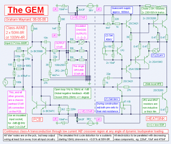
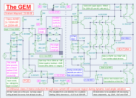
The GEM is an audio power amplifier embodying simultaneously active Class A and Class AB output stages for 100+ Watts into a 4 ohm loudspeaker. The front end pcb will drive up to 100+W variants, or the 200+ Watts version into a 4 ohm loudspeaker load.
Notes:
The circuit for this design developed out of some 35 years of on/off investigations into the John Linsley-Hood, MIEE, 1969 class-A amplifier. It has been named in remembrance of my late father, Gordon Ernest Maynard, who supported my interest in audio/electronics/radio/etc. from a young age. It is not claimed to be the best amplifier for anyone to use, for indeed there are so many system design ideals and requirements that not one of them can be expected to suit everyone, no matter how well any one might measure and perform in relation to original requirements. As always there is more than one way of studying any problem and achieving a given end result.
The original and 'simple' 1969 JLH class-A amplifier design provides excellent first cycle accuracy through mid and high frequencies, thus its delivery is both neutral and clean. Being class-A there are no output stage conduction crossovers, and, if properly constructed there is no need for the stabilisation components or the series output choke that so often introduce NFB control delay to a real world amplifier's output terminals when dynamic loudspeakers are being driven. The JLH not only amplifies percussion transients and spoken sibilants cleanly, it is also silent behind voices and notes, such that an artificial brightness or smear does not affect the reproduction of detail, and thus its output is instantly recognisable as being correct. So many 'distortion' analysts study an amplifier's forward linearity characteristics under steady sinewave drive with a passive resistor load whilst ignoring the complex circuit activity that arises when dynamic loudspeakers are driven by dynamic and asymmetric music signal waveforms. The JLH amplitude 'distorts' more than most amplifiers under forward analysis, and yet it sounds much better because of the way its circuit damps without delay or overshoot in the presence of secondary dynamically generated loudspeaker system back-EMFs which attempt to reverse drive the output terminal.
For more in-depth information and construction details about JLH class-A amplifiers, see Geoff Moss's excellent Website:-
http://www.tcaas.btinternet.co.uk/index.htm
The two most significant reasons for a JLH class-A amplifier presenting a sonically neutral output relate to it having an open loop bandwidth adequate for audio requirements *before* NFB is applied, then to it possessing a natural closed loop stability without need for additional dominant pole filtering which might then infringe upon those open loop capabilities; hence the closed NFB loop's ability to maintain phase linear control of output terminal potential in the presence of loudspeaker generated back-EMF up to the very highest of audio frequencies.
So often it is a need to add stabilisation components to other amplifier designs where NFB is used to reduce amplitude distortion, that leads to these very same components introducing a NFB delay which then colours dynamic loudspeaker reproduction in a manner steady sine measurements simply cannot ever reveal. This colouration arises when output stage driven amplifier-loudspeaker system current flow becomes back-EMF modified by the dynamically induced milli-second to milli-second variation of reactive loudspeaker system elements, as their impedance and phase angle change due to the momentary sequential elemental delays related to storage and release of audio waveform energies. If loudspeaker current flow becomes leading with respect to audio amplifier input waveform voltage, and the necessary correcting NFB loop response is fractionally delayed by a bandwidth limiting dominant pole filter or internal series output choke, then the amplifier's output current correction becomes lagging at higher frequencies and the output terminal cannot quickly enough be prevented from developing a fractional error potential. The amplifier does quickly 'catch up', but in the meantime a tiny additional loudspeaker system dependent 'dominant pole and/or choke related' interaction error has already been generated at the amplifier-loudspeaker interface, and no amount of NFB can completely erase this because it was NFB control delay with respect to priorly energised loudspeaker back-EMF that caused it in the first place!
So why then does not everyone use good JLH, Nelson Pass or other class-A amplifiers ?
(1) They run constantly hot when compared to other amplifier types.
(2) Pure biased class-A designs lack dynamic powering capabilities.
(3) Some provide marginal low frequency phase response or damping.
STEPPING STONES.
During the early 1970s I constructed a large JLH class-A monoblock. It had a genuine 100W measured sine output, sounded very clean, and could generate surprisingly noisy short circuit sparks to raise thoughts about output stage survival. (It never blew, and still runs!) However when it was compared with a physically smaller and cooler running 2x KT88 Ultralinear Leak TL50+ this solid state monster lacked dynamic attack. It also sounded like a purely voiced but wimpish choirboy when beside the maturely rocking muscle outputs of other typical 100W class-AB solid state chassis.
The reason for this 'weakness' relates to loudspeaker current flow, whereby dynamically induced momentary requirements can far exceed the peak sinusoidal output capability of a pure class-A biased output stage. This, combined with an inability for the JLH upper output transistor to conduct as deeply as the lower transistor, leads to what sounds like a pop-rock music output linearity weakness developing as soon as half power levels are reached. With modern H-pak plastic power transistors it is possible to obtain up to 50W of pure class-A output from a single pair of JLH connected output devices, but there will still be that positive going output current limitation when the amplifier is used to drive dynamic loudspeaker systems.
I returned to this problem many times, and at first attempted to overcome it by upping the class-A rating whilst implementing different dynamic biasing arrangements to hold down the quiescent dissipation. These designs worked, and I achieved 100W of class-A output for 100W of quiescent heat. Generally though the resulting amplifier was not temperature stable through different audio duty cycles; or their biasing arrangements had an audible impact upon transients; or they were unacceptably complex.
More recently I tried numerous arrangements where individual output devices were replaced by identical composite sub-circuits running in class-A at low level, though conducting as if class-AB during periods of increased output demand. This type of arrangement simulated well, they also worked and were less complex than with additional biasing arrangements, but they sounded 'punchy' as if the amplifier was over reacting to loudspeaker generated back-EMFs; as if the phase splitting JLH driver could not maintain balanced drive splitting control when the individual composite output device dynamic characteristics became externally altered on a per-half basis by varying loudspeaker system demand.
A NEW CROSSING.
More recently it occurred to me that the JLH current splitting transistor *collector* could be used to drive a conventional class-AB output stage, whilst its *emitter* controlled a lower JLH class-A output device exactly as before. Also the upper half of that class-AB output stage could then simultaneously be used as the upper half for the lower class-A output device; in other words, both class-A plus class-AB output stages in one circuit, with a common output termination, each operating simultaneously, with the class-A connection maintaining transconduction continuity through low current class-AB crossovers at no matter what voltage angle any loudspeaker current might momentarily flow.
Now this did work, and well too, but I was still not convinced that the sound could hold its own against good tube power amplifiers, so I was still not able to hang up my imagineering hat. I reasoned that further improvement would be possible through providing a 'stand alone' upper half class-A collector load in order to fully separate class-A current flow from the class-AB biasing arrangement. My options for this were resistors, a transistor current sink, or an output choke similar to those that went out of fashion long before transistors were invented!
Now resistor current flow between the positive rail and the class-A collector could not remain constant through large output voltage amplitude swings; this means that the A-AB bias balance would be correct at zero output potential only, and whilst adequate for high quality at low output levels only, bias interaction would increase through loud asymmetrical music waveforms; also the resistors could not be bootstrapped due to their need for low value. Transistor current sinks can introduce their own amplitude/slew induced non-linearities plus an inconstant reference bias variation with temperature, this resulting in a quiescent A-AB bias null offset variation with temperature. An output choke is simple and realisable, and although winding heat dissipation would be a problem I still felt that this option could be successfully implemented. As indeed it was for the 100+W version. However additional heat dissipation from a choke suitable for the 200+W version would require this component to being specially wound, so although I had a perfectly functional base design my thinking was still not over. Eventually I realised that the VAS bias chain could simultaneously set the reference potential for a positive rail based current source, as is shown in the higher power circuit. Both of the above circuits have been fully tested, thus either the choke or transistor constant current source class-A output stage option may be chosen.
So now, and at very - very - long last, I actually have a most capable solid state 'audio' power amplifier that is capable of the low level refinement normally available only via genuine class-A amplification, yet with equal refinement throughout its excellent high power class-AB drive reserve, plus, and this too is at all levels, a 'blackness' behind notes and voices that is more often associated with top flight tube amplifiers only. Some might say it is the silence between the notes that makes a performance, but when it comes to audio reproduction it is that lack of cerebral distraction due to the silence behind the notes, which then allows us the pleasure of imagining ourselves as being 'live' at the recording performance.
KEEPING DRY
I have always studied music waveforms from a dynamic viewpoint - as if they are an irregular series of 'splashy' and ever changing asymmetrical first cycles; not the smoothly liquid streams of sinusoidal components that theoreticists so often encourage us to dip and waggle our toes in whilst we are encouraged to follow their academically correct but time isolated examination methodologies. Unless our thoughts stay with initially coherent audio wavefronts and the turbulently reactive myriad of circuit and interface responses subsequently arising, simplistic applications of established theory can so blinker that we become distracted from more meaningful fundamental matters.
It is here worth noting (1) the original JLH class-A has no additional signal or NFB path capacitance capable of delaying transient response capabilities, also, (2) the integral NFB cannot become positive at a high frequency because of the tailored overall gain-bandwith product with so few active devices being enclosed by the NFB loop.
Of particular importance is that NFB is applied to the emitter of the first transistor with respect to the input base plus any audio input carried thereon. This is a classic series connected voltage feedback arrangement. So, although the JLH class-A has two distinct 180 degree phase changes along its signal path, both of these are not then encompassed by the closed NFB loop, and this is why with sensible construction topology and loading, these amplifiers cannot splash over into device induced phase shift instability at higher frequencies. The high frequency output voltage does not become fully out of phase with potential at the input transistor *emitter*!
Unfortunately any circuit more complex than the basic bipolar JLH class-A naturally introduces additional high frequency phase change, whether this is through Mosfet gate capacitance or the utilisation of additional bipolar devices. Generally there is then a need to compromise between stability and open loop bandwidth control, and this can end up audibly impacting upon first cycle (transient) response capabilities.
Thus, opting to use a differential input stage in order to minimise input transconductance distortion and output zero offset drift; or, mirroring the differential input stage to reduce power-up thump and maximise open loop gain plus NFB - which further minimises amplitude non-linearity; or, running an output stage using Mosfets or separate drivers and output transistors; can, individually or together, be said to introduce 'audible' change - if - the dominant pole turnover frequency must subsequently be pulled down to, or be reduced to a lesser open loop audio frequency in order that closed loop stability be ensured.
Yet I implement all three of these individual circuit arrangements whilst still retaining excellent first cycle and signal to (noise + control delay induced error) figures, plus good stability and low distortion. It is fact that a good total harmonic distortion specification cannot guarantee a good first sinewave cycle response because sine measurements are not taken until after the first cycle has passed and the waveform has become steady; whereas a low first sinewave cycle distortion figure cannot be achieved without the overall thd. figure already being better at the same frequency.
AVOIDING SPRAY.
To overcome additional semiconductor device induced phase change at high frequency I implement a base emitter connected 10nF capacitor at the differential input pair NFB sensing node, plus a 220nF base-emitter connected capacitor on the NFB leg of the differential mirror. These values are chosen to have minimal impact upon the forward audio frequency signal path with regard to the established tail current plus output stage loading of the differential pair. At higher frequencies however, where additional device usage could introduce unavoidable phase changes within the closed NFB loop and cause closed loop instability, these capacitors make the differential pair behave like an original single JLH input transistor with series emitter voltage feedback, and make the current mirror behave like an inactive current source!
The separate but simultaneously driven and parallel output connected single ended class-A output stage actively minimises inherent transconduction variation and switching delays through the relatively low current class-AB crossovers at moments when a dynamic loudspeaker load presents the output terminal with leading load current (momentary reverse current drive). Additionally, the local, plain 27k resistor derived, A//AB output stage degeneration sets up a constant minimum of crossover error damping without reliance upon the global NFB loop! The output stage is further additionally stabilised in its own right via a Miller connected 22pF plus 1k series capacitor-resistor pair at the VAS/splitter transistor, yet again though, using component values which cannot impact upon the open loop audio bandwidth. With higher rail voltages and twice the number of output devices used in the 200+W circuit, these values become 47pF and 470 ohms, though when equivalent / fake / non-Toshiba / older devices are used, then the Miller connected values should become 47pF + 1k for the 100+W, and 100pF + 470 ohms for the 200+W circuits.
Overall then, if this circuit is physically constructed using the recommended star ground, star rail and star output nodes which prevent current peak induced hf voltage drops along the connector to one sub-circuit interconnect from co-coupling into another, the resulting GEM amplifier will present a low and flat phased output impedance which renders it highly impervious to composite dynamic loudspeaker system impedance variation and the back-EMF induced interface errors that can so often arise with global NFB amplifier designs due to their dominant pole filters delaying output current generated control of output terminal voltage.
In spite of what some designers claim, there is no way of completely eradicating or displacing crossover distortion arising when a lone class-AB amplifier dynamically drives a reactive loudspeaker. NFB might reduce the resultant load induced distortion, but cannot fully eradicate it because loudspeaker back-EMF generated currents can reverse drive the class-AB output stage through a fraction of its crossover bias potential before dominant pole delayed NFB control can attempt correction. When the dominant pole is at an open loop audio frequency, the effect upon the closed loop response becomes audible because the control of loudspeaker generated back-EMF becomes phase shifted, and thus fractionally delayed, with a new additional momentarily uncontrolled output terminal voltage error arising that has nothing to do with the original input signal waveform. Thus output terminal voltage error generated due to say a bass or mid driver section back-EMF can become directly coupled into mid and tweeter drivers.
It is loudspeaker system current flow causing the development of these output terminal error voltages which the amplifier cannot quickly enough prevent, that then becomes recognisable as a typical 'solid state sound'. This often manifests as a falsely bright, occasionally a more desirable 'live' response, a perception like 'glassy' or 'ice cold', a jittery high treble, or occasionally as an uncomfortable upper mid-range peak. It can 'inexplicably' arise after a set of loudspeakers has been changed, yet actually be due to flawed amplifier design! Thus there is considerable difference between designing an amplifier capable of amplifying audio frequencies at low distortion when resistively loaded, and designing an 'audio' amplifier capable of competently driving real-world loudspeaker systems! If you doubt this statement, then please compare in a directly switched A-B fashion, this class-A//AB amplifier with other conventional class-AB types.
THAT'S IT!!!
During the 1970s the Quad Hi-Fi company patented their '405' Current Dumping design. It was powerful, good sounding, compact and reliable. I used one myself and marvelled at their theoretical ingenuity, though for me the 2x KT88 Leak TL50+ still provided better reproduction. Since then that Current Dumping circuit has been repeatedly refined for professional or home use, and yet whilst updated models remain available today, so does a more recent Quad 2x KT88 II-40 monoblock chassis! The Current Dumping circuit cleverly combines both class-B and class-A output stages through a reactive output bridge which allows for the slower class-B switching. With my own circuit however, I have combined class-AB and class-A outputs in real time, this to provide powerful audio reserves with a class-A like cleanliness, whilst retaining the kind of transparency at higher output powers more often associated with expensive push-pull triodes or those ultralinear kinkless tetrode (KT) designs. (Prior to this my favourite power amplifier had been my own hybrid 100W 4x KT88 UL PP-AB1). I also believe the performance of the GEM is future proof and will not be superceded by digital amplifier designs, because dynamically energised loudspeaker system back-EMFs cannot fail to interact with the integral filters necessary to prevent their switching output stages from becoming RF noise transmitters.
CONSTRUCTION NOTES:
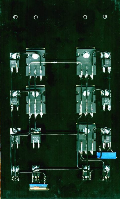
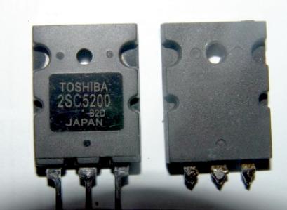
This circuit was intended for use with modern 2SC5200-2SA1943 power transistors, yet it has been successfully constructed using other device types, including a single Sanken 2SA1216+2SC2922 pair in place of the paralleled 100+W AB outputs. Feel free to use whatever transistors are to hand or in your 'salvage' box because the parallel class-A plus class-AB operation will make better use of obsolete / scrap devices than can conventional amplifier circuits, including the old and almost indestructible industrial 2N3055 based series.
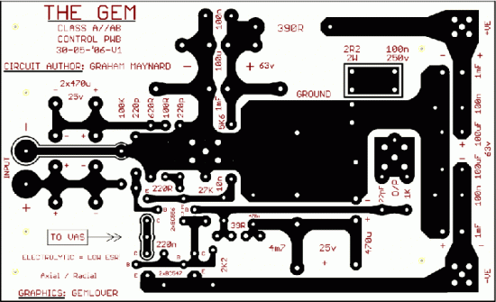
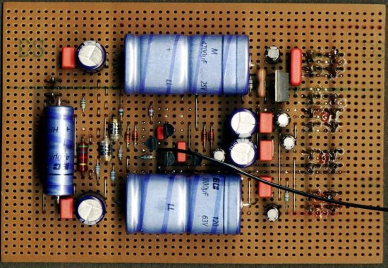
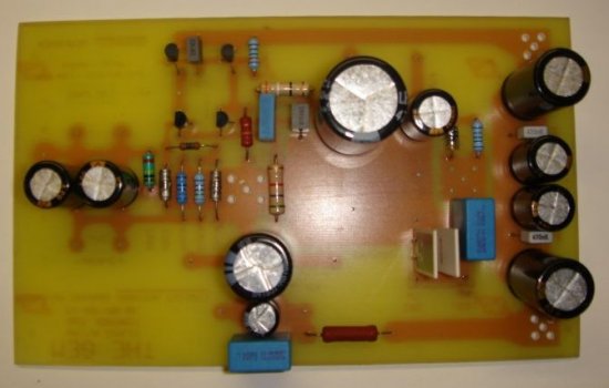
Keep VAS, Zobel and output related wires at least 5cm/2" away from input devices and wiring. Use a star earth, star power distribution points from each fused psu rail low ESR 10mF at the pcb, and a star output node connection. It is also essential to use separate wires between the negative star node, the PNP output collectors, and the class-A emitter resistor to prevent class-AB current peaks from voltage modulating the class-A stage via wire impedance. See the illustrations for a universal pcb layout kindly contributed by Daniel Bosch in South Africa. This board has been designed to use any locally available axial or radial capacitor types, including larger low ESR variants. Parallel all of the large electrolytic capacitors with lower value components to minimise the risk of effects due to an unexpected series impedance peak. Do not twist any extender e-b-c wires used to connect out to heatsink mounted output stage devices. Mount the VAS, the drivers, also the Vbe multiplier on the output heatsink for automatic temperature compensation. During assembly check/adjust the pre-sets sliders for 50% setting; note that these should be 15 or 10 turn components. If long wires cannot be avoided with your choice of layout, then fit additional 1uF capacitors between each class-AB output device collector and the heatsink ground. The series input capacitor comprises two 470uF components in parallel, though mutually connected plus to minus, my own being low ESR types.
I recommend, after checking the circuit wiring for correct assembly, first powering up using two 9V transistor radio batteries, then with 22 ohm per rail power resistors in place of the fuses as protection for any error at initial switch-on. However, do not try to set any bias with either of these testing options. If everything is okay the amplifier should present an unbiased open circuit zero output potential within 100mV. It should also cleanly drive a test loudspeaker for low level signal testing without any bias being set up, as the two amplifier output stages will automatically compensate for each other's lack of bias; you should not hear anything through the loudspeaker after a possible low level initial power-up charge. I suggest your testing input could be taken from the headphone output of a portable CD player or an i-Pod, whereupon the unbiased amplifier should produce limited audio, even on rails as low as +/-9V!
PCB Layout
If all is well, power up with a fully fused psu connection. Clip a pair of test multimeter wires to class-AB output emitter resistors as indicated on the circuit diagram. Slowly increase the value of the class-A bias trimpot until the class-AB 'imbalance' reading nulls to zero; then adjust the class-AB trimpot for an average 40mV of quiescent bias per output pair. Re-set the bias from zero current after two hours of normal use.
For 70W/4R=2x35W/8R use 30V rails. For 50W/4R=2/25W-8R use 25V rails with just a single pair of class-AB power transistors. Daniel has my thanks for checking out every modification update as it arose, whilst running his 200+W GEMs to drive Apogee loudspeakers throughout the last 12 months.
Always re-bias from zero current if you alter the rail voltages. If necessary insert a 0.22 ohm resistor in series with the output terminal to maintain stability when driving capacitively reactive loads, or use any series output resistor value up to 2.2 ohm if you wish to imitate different types of tube power amplifier output impedance and damping. Also don't forget to bi- or tri-wire out to composite loudspeaker system sections and drivers in order to obviate single cable developed dynamic voltage drops due to varying crossover-loudspeaker system generated back-EMFs, no matter how expensive your loudspeaker cable might be!
Better still, use these amplifiers as they are intended - as line driven and loudspeaker sited monoblocks! A simple line driver circuit appears on another page, this may be used to buffer the output of a tube DAC or pre-amplifier, or be combined with the GEM amplifier to raise its stand alone input impedance. Pcb outlines are also shown.
Finally and very importantly, in relation to the single ended output choke option!
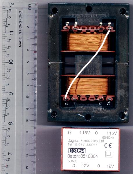
Whilst it is possible to run this amplifier without any choke, say by series connecting four 22 ohm heatsink mounted resistors in its place, for the lower power version I use two 230V 50VA mains transformers primaries connected in series. These have a resistance of approximately 40 ohms each, and do become rather hot, so free air ventilation is essential. My transformers were cut apart, then re-assembled as a thick paper gapped twin 'E' core assembly. See photo.
Circuit Images
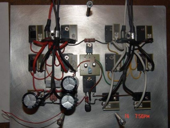
The links below are all pictures of the actual prototype. Some of these images are quite large and may be resized automatically to fit in your browser. Clicking on the actual image restores full size or images can be saved by using a right mouse click.
Fake Transistors
Beware of fake Toshiba Transistors. The genuine article is shown below on the left. The center and right most image are fake Toshiba transistors. The fakes have higher junction capacitance and limit the high frequency response having an adverse effect on sound quality.
WARNING !
Do not manually attempt to connect or disconnect the output choke once this amplifier has been powered up. If you are holding the connecting wire and the wire insulation breaks down under back-EMF potential, it will not be the amplifier that is damaged, but *YOU*.
My Conclusion
I have enjoyed music listening through several fine amplifiers, but for me this development supersedes all because it imparts notable loudspeaker control without generating the secondary amplifier-loudspeaker interface current flow related error components which so often spoil solid-state amplification.
Thus I wish everyone who constructs this GEM - the very best of listening....
..... Graham Maynard.

